ENGR 2705 - Lab #14
Title:
Simple Processor
Objectives:
- Gain further familiarity with the state machines
- Design and implement a simple processor
Parts:
- PC running Quartus II
- Altera DE2 Board
Background:
Transmission of data between two devices often requires "handshaking" signals to ensure the data is received correctly, especially when the two devices run at very different speeds (clock frequencies). For example, if n bits of data are to be transmitted from Device #1 to Device #2 as shown in Figure 1, Device #2 raises (asserts) the Data_Request signal when it is capable of receiving new data. Once Device #1 sees that Data_Request is raised and it has placed correct data on the n Data lines, then it raises the Data_Ready signal. After Device #2 has taken the data (typically stored in a register) from the n Data lines, then it will lower (unassert) the Data_Request signal. Device #1 can lower the Data_Ready signal only after the Data_Request signal has been lowered. Device #2 can only make a new request after the Data_Ready signal has been lowered. This is known as a "full handshake" and ensures that the data is transferred correctly even when the two devices are running at very different speeds. For this lab you, the human user, will be Device #1 and the state machine running at 27 MHz, that you will develop, will be Device #2.
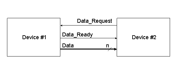 |
| Figure 1: Handshaking |
Procedure:
- Create a 3-bit register using D Flip-Flops that has a Reset input and an Enable input. Both should be active high. Verify your register works correctly by perfoming a functional simulation. Create an appropriate symbol for the register.
- Create a 3-bit unsigned adder that has a Cout output. Verify your circuit works correctly. Create an appropriate symbol for the circuit.
- Have your design for a seven-segment display driver from Lab #6 available including a symbol. If your circuit did not work correctly then correct your circuit or get a working copy of this circuit from another student.
- Use the graphical editor to produce the circuit in Figure 2. Simulate the use of this
circuit to add two 3-bit numbers, applied one at a time through input A.
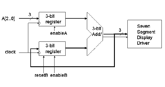
Figure 2: Processor Datapath - Design the finite state machine shown in Figure 3 that controls the circuit of Part
4, and interacts with you, the human user. The clock signal for the state machine
and for the circuit from Part 4 will be connected to the 27 MHz clock signal that
is provided on the DE2 Board. The state machine begins operation when the Go input is asserted. It begins by requesting, via handshaking, two 3-bit unsigned numbers
from the user, one at a time. It adds the first number to the second number. Also,
provide a negative logic master reset input that causes the machine to go to the beginning
state. Implement the state machine in Verilog. Make sure a symbol is created. Simulate
the machine to verify it works correctly.
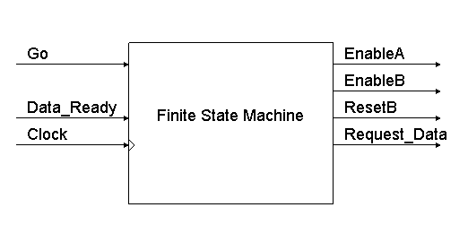
Figure 3: Processor Control - Create a final circuit using the graphical editor by combining the circuit from Part 4 with the circuit from Part 5. Simulate the circuit to verify it works correctly. Also perform a timing simulation and report the worst case delay.
- Use a debounced push-button switch for both Go and Data_Ready signal. The push-button switches are active low so you will need to add not gates for Go and Data_Ready to your circuit.
- Download the final circuit into the DE2 Board. Verify the circuit works correctly. Record results in your lab book. Show your working circuit to the instructor.
Conclusions:
- Discuss how well the objectives were met.
- Discuss what you learned.